PCB Designing and Fabrication
To be graduated i was required to make a custom PCB for my electronics ,which can be used to take input , can provide output , and also can do networking with other systems also
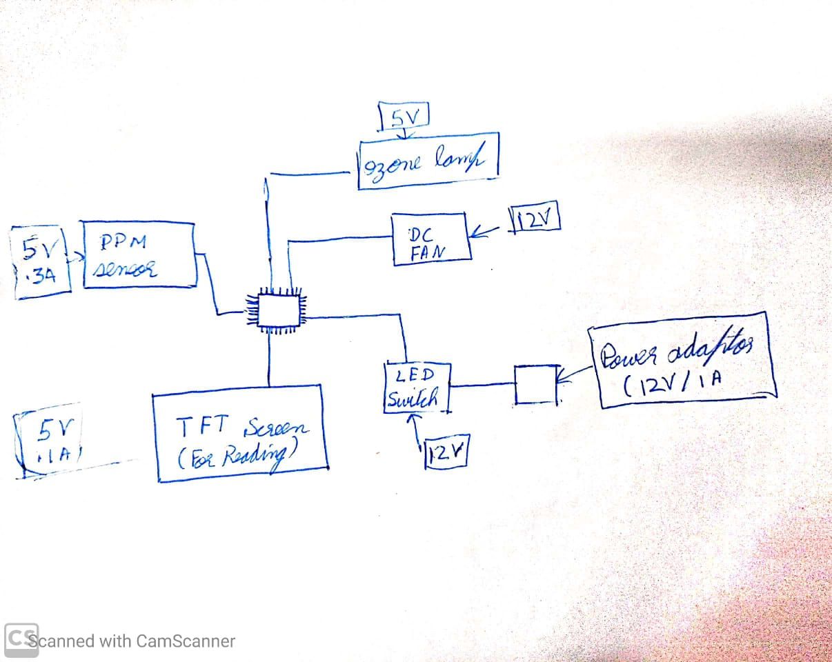
First before going to design something i was required to make a rough schematic like , what will be connected to what , and what are there current requirement as well as on what voltage they work
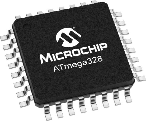
I used Atmega 328p as my main Ic
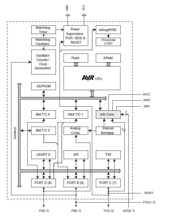
I have explained about this I.c in detail on this page , if you ike you can go and
see how it works and what are its pinout
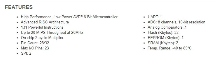
Basic feature of ATMEGA 328P , well the main decision of my choosing this pcb was that , it was easily available in ur lab as well as it the same chipset use in Arduino UNO.
Satshakit
well before i never desined PCB and to start i look to this satshakit , it is a atmega 328p based pcb which was ddesigned by previous year students , with a detailed documention if you like you can go on the original page by clicking on this link
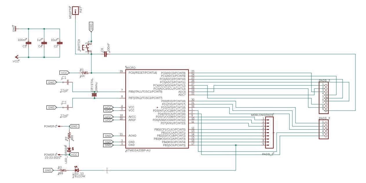
This is the standard schematic of satshakit
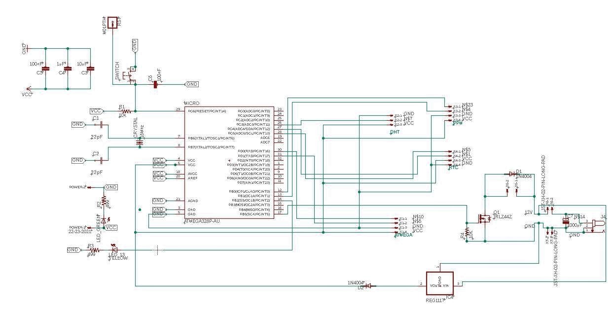
This is the schematic for my PCB
this is my board which i cutted initialy , but i accidently forget to add avrisp pins and without those pins i won't able to program the board , so ineed to add those pins
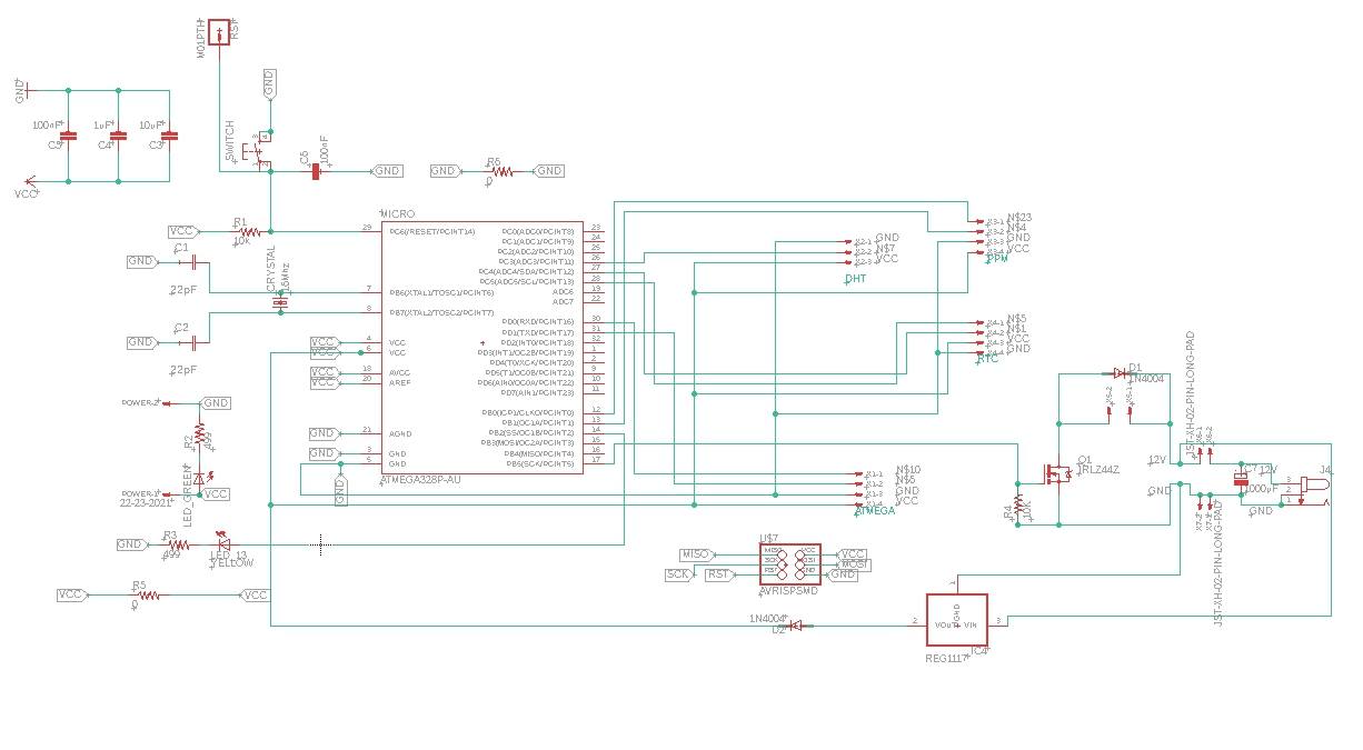
This is my modified schematic which has Avrisp pins which i want
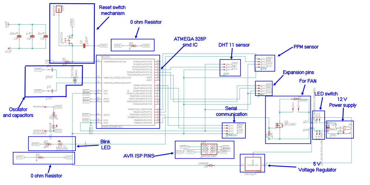
I have in detail explained my schematic
So i modified my board to incorporate those pins as well
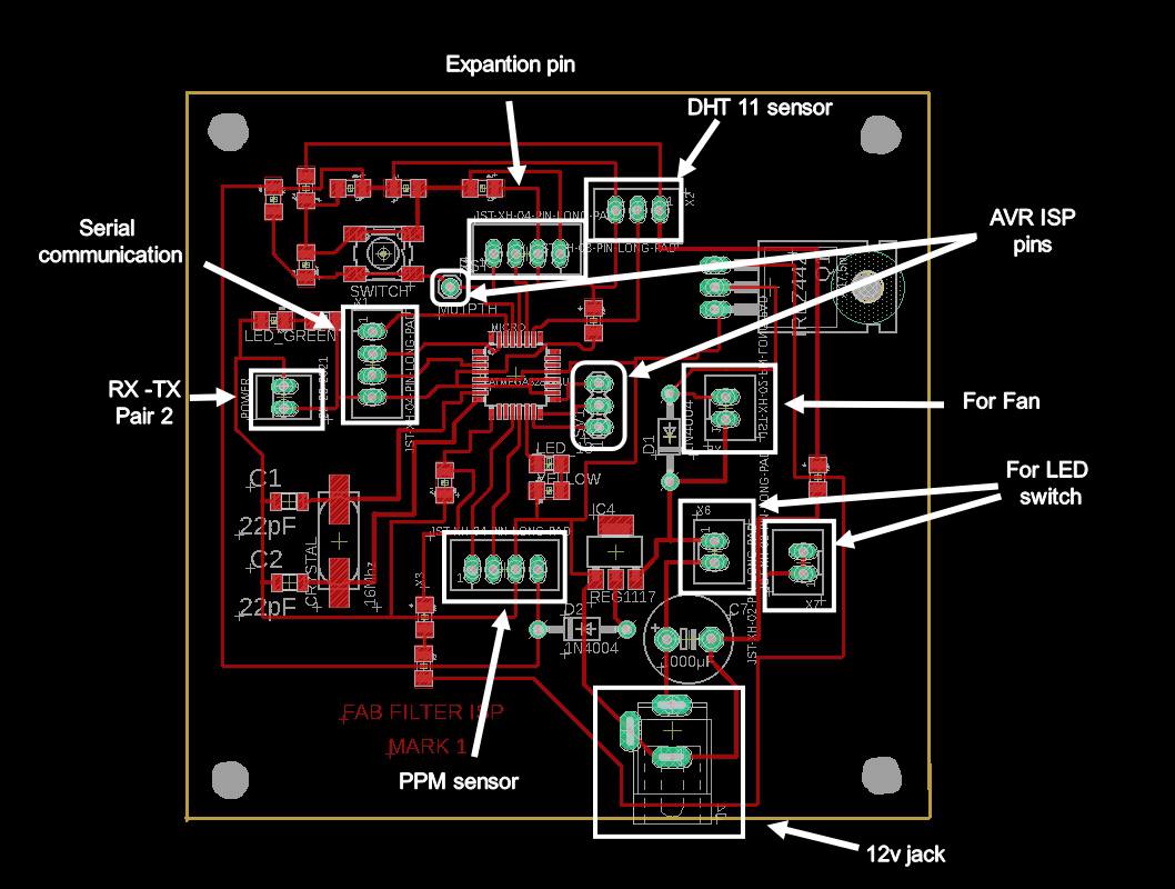
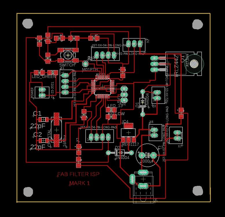
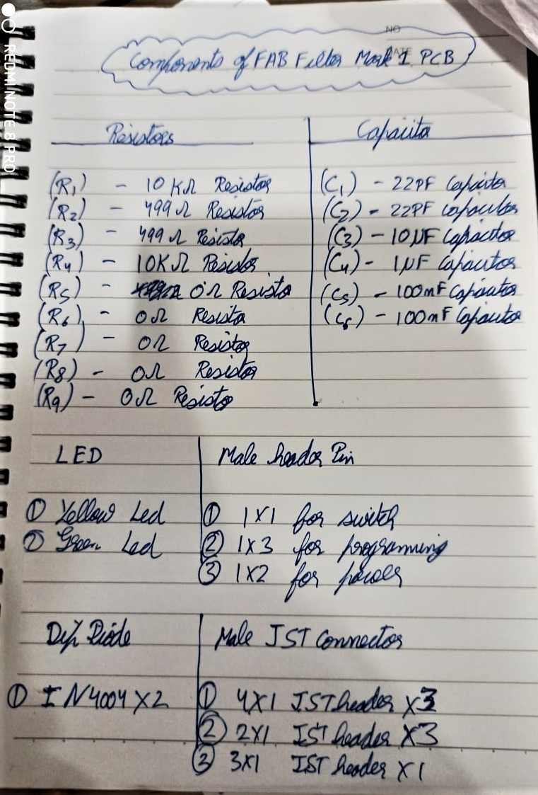
Throught this image all the components of my board
I am attaching all the CAD Files here if you want you can download these files
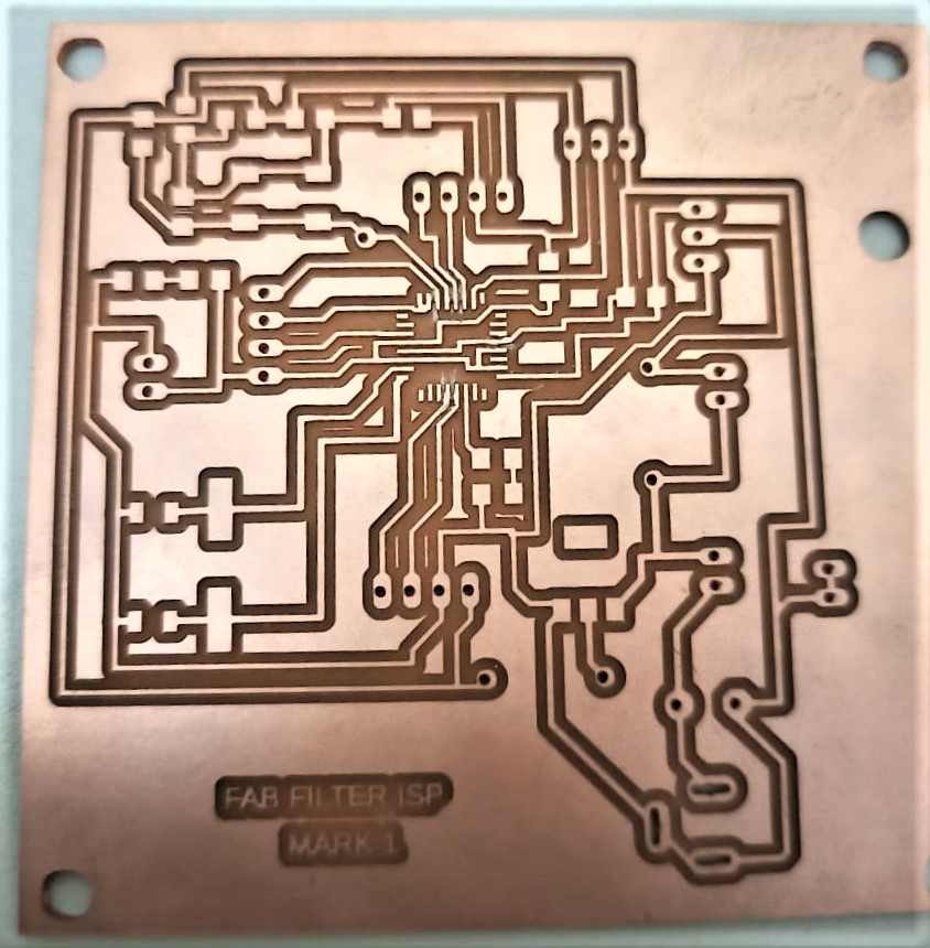
FAB Filter Mark 1 isp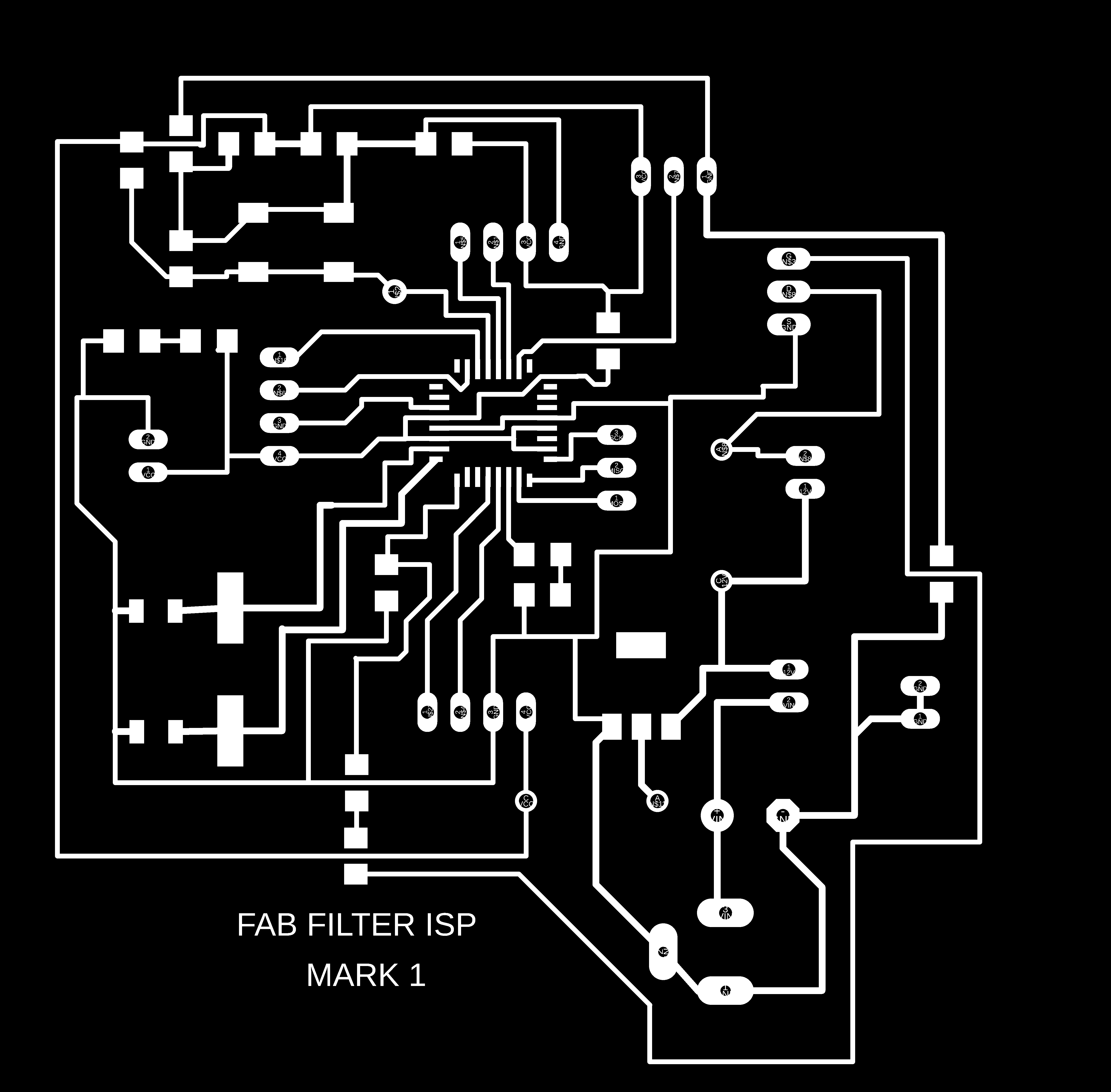
This will be png image for my pcb track which will be milled in srm 20
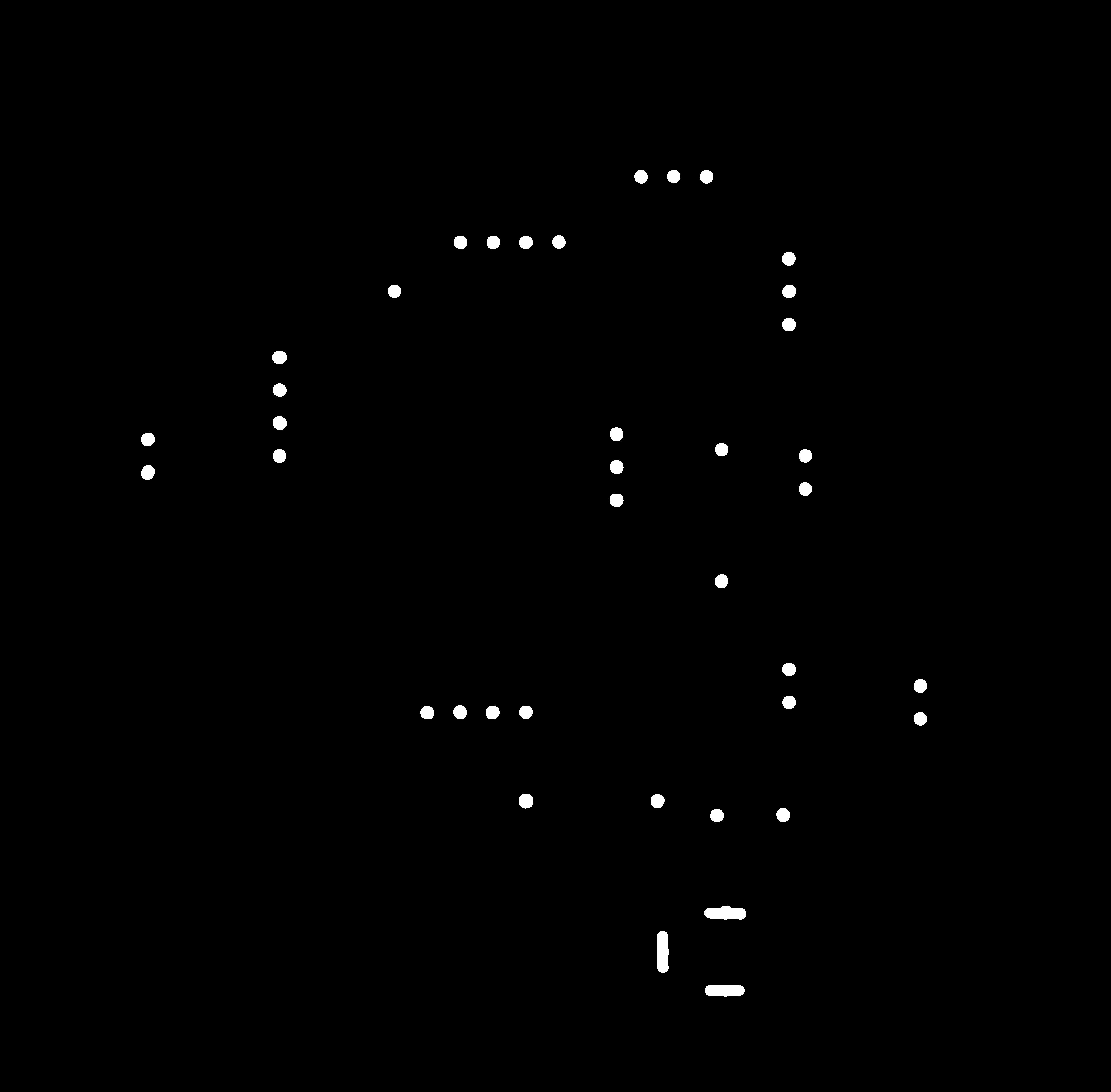
Holes for through holes components , please dont forget to invert the the image befor making .rml file
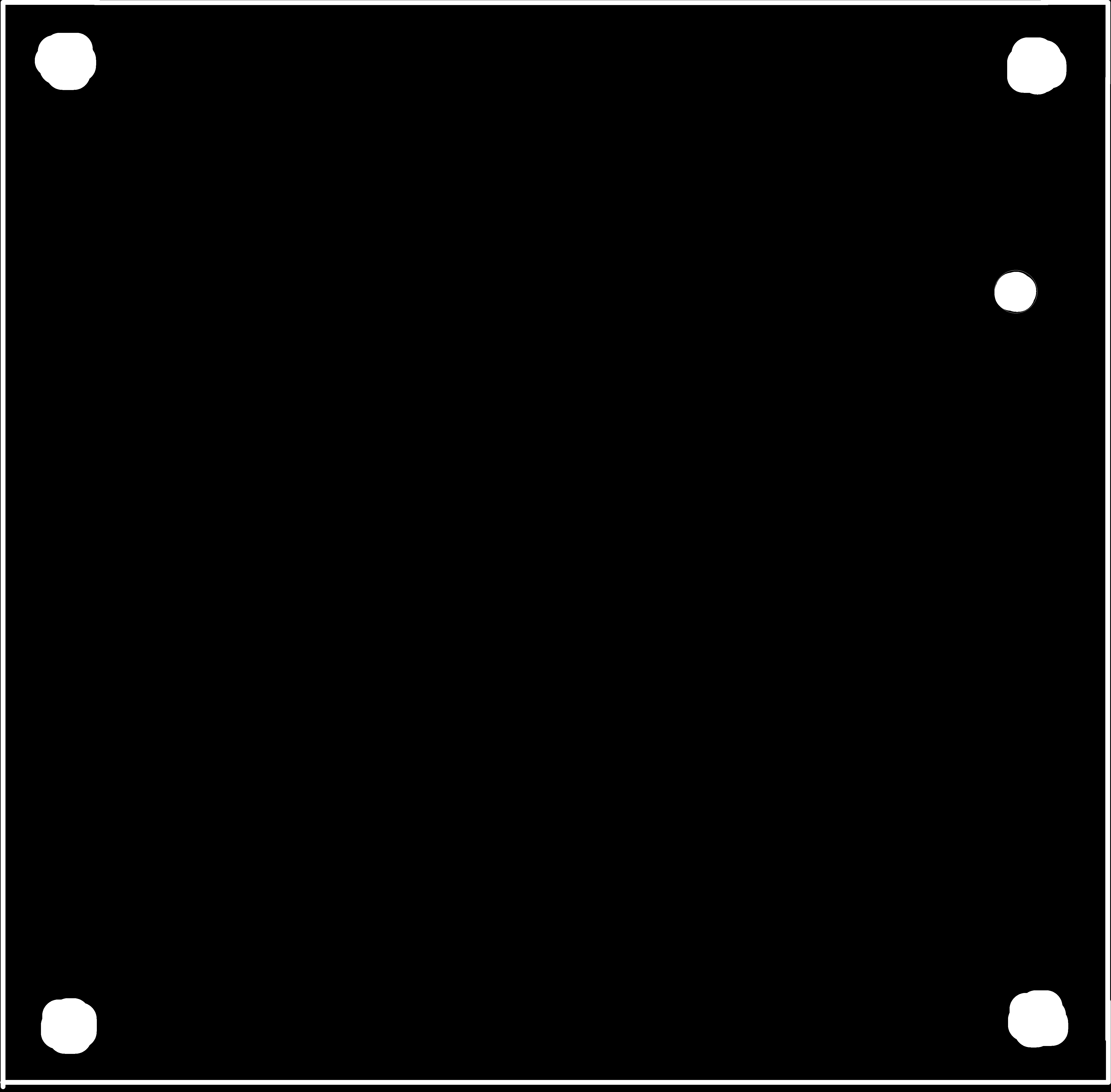
This is for border or you can say cutout part
Timeleapse video for pcb milling
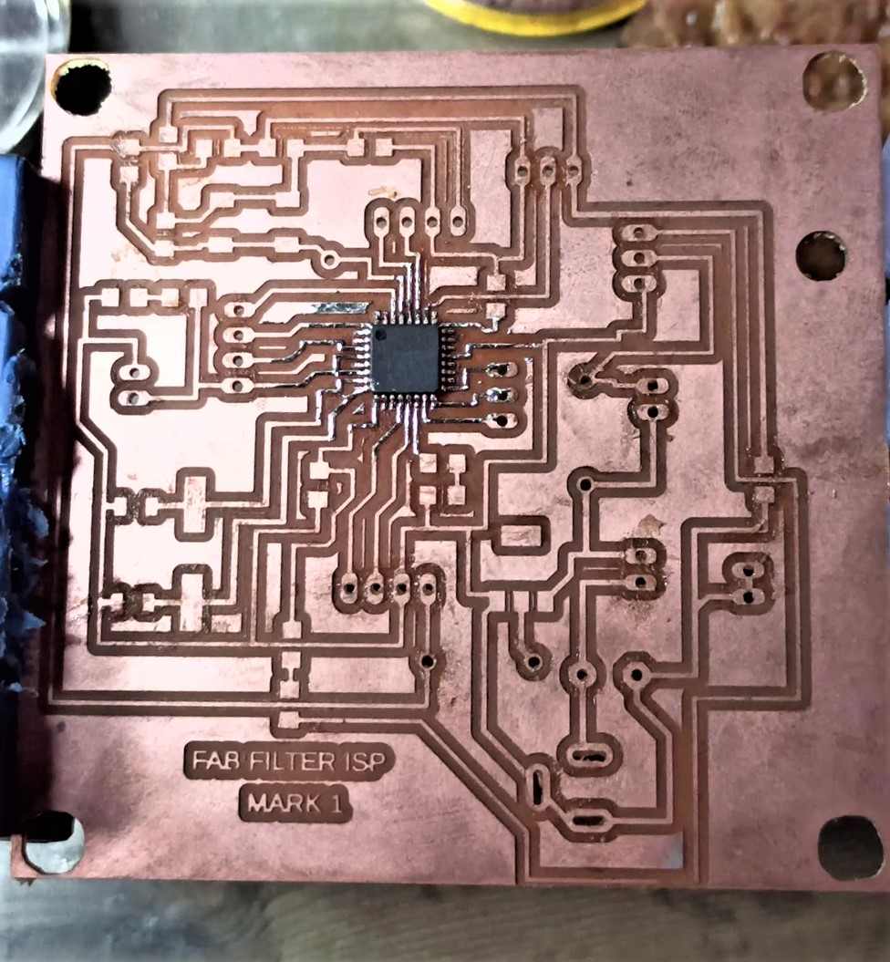
Finally got a pcb
Time to start soldering
A important word of advice make a list of components required for you pcb and take them our and marked them in line , it will save a lot of time an keep the working pace
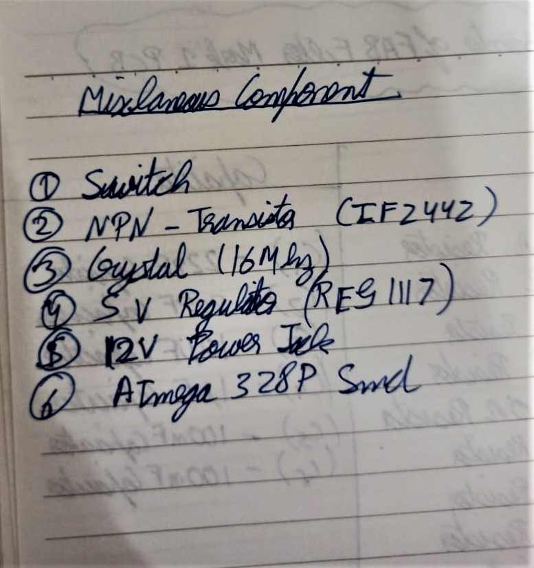
Like i said brought ought all the components according to my list and then start soldering them in the same manner
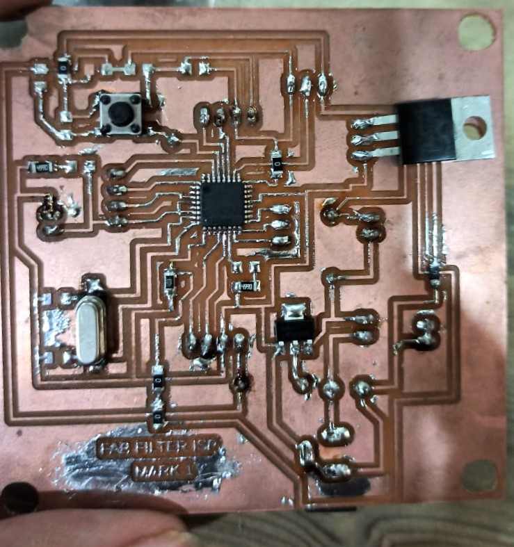
This is partially soldered pcb
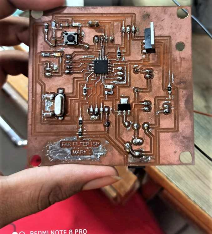
This is fully soldered PCB , and i dont understand why when i finished soldering all the components my PCB looks like crap
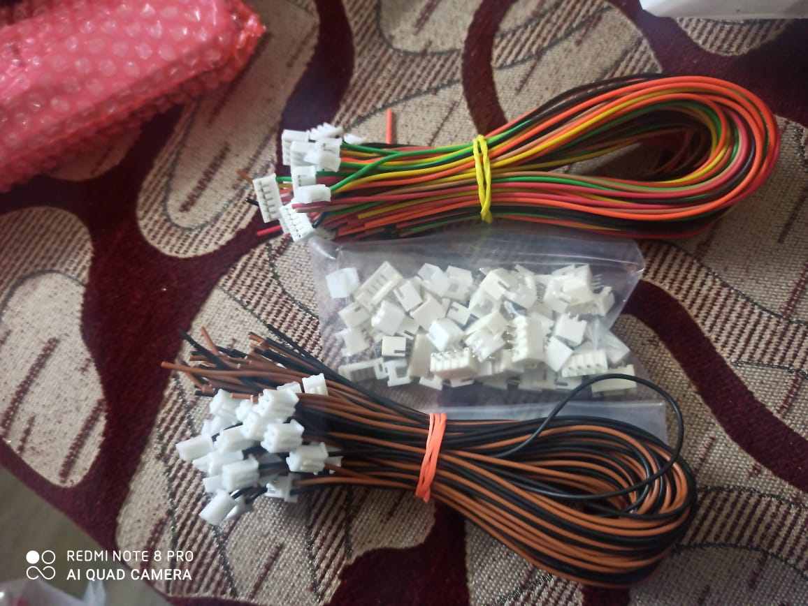
Rather then using the same jumber wires for connection we preferred to go with JST connectors as , you can through this image , and we easily get ther track for eagle ,the main purpose of doing that was to eleminate those loose jumper wire's
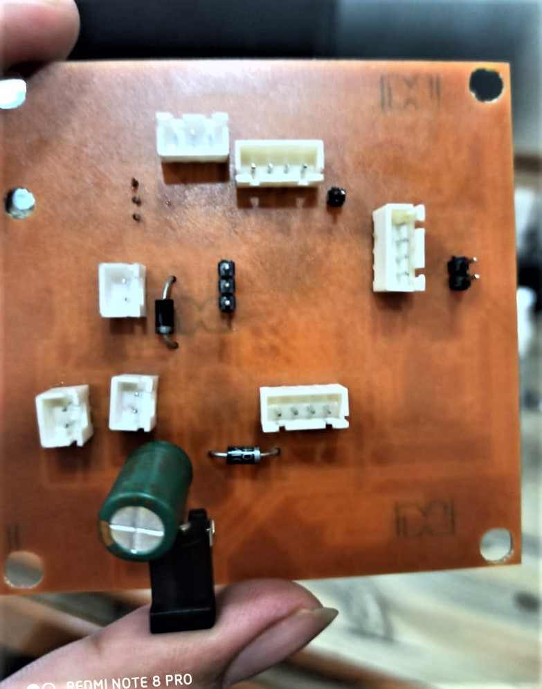
Through this image you can see how we only have those JST connectors only and we preffered that way
If you like to know how iprogram my board pls click on this link , it will guide you to my embedded programing page